« home

MOSFET

physicselectronicssolid state physicscetztikz

The metal-oxide-semiconductor field-effect transistor, or MOSFET for short, is the most frequently manufactured device in history, with close to 10^23 MOSFETs produced since 1960. As the basic building block of almost all modern electronics, it revolutionized the world economy and triggered our ascent into the information age.
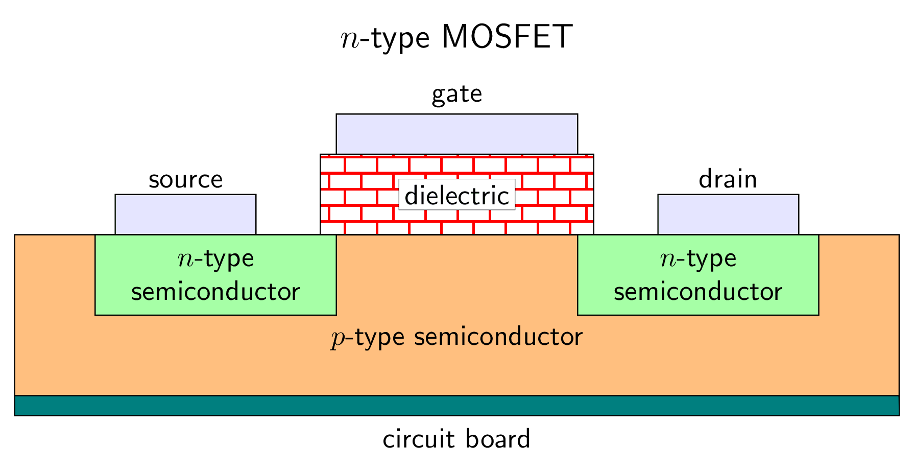

MOSFET

  Download

PNGPDFSVG

  Code

  LaTeX

mosfet.tex (24 lines)

\documentclass[tikz, border=5pt]{standalone}

\usetikzlibrary{patterns}

\begin{document}

\begin{tikzpicture}[font=\sffamily]
  \node[above=1ex] at (2,3.5) {\large $n$-channel MOSFET};

  \draw[fill = teal] (0,0) rectangle (11,-0.25) node[below=1ex, midway] {circuit board};
  \draw[fill=orange!50] (0,0) rectangle (11,2) node [below,midway] {$p$-doped semiconductor};

  \draw[pattern=bricks, pattern color=red] (4-0.2,2) rectangle (7+0.2,3) node[midway, fill=white, inner sep=2pt, draw, ultra thin, rounded corners=1] {dielectric};

  \draw[fill=blue!10] (4,3) rectangle (7,3.5) node[above=6pt, midway] {gate};
  \draw[fill=blue!10] (1.25,2) rectangle (3,2.5) node[above=6pt, midway] {source};
  \draw[fill=blue!10] (8,2) rectangle (9.75,2.5) node[above=6pt, midway] {drain};

  \foreach \x in {1,7} {
    \filldraw[fill=green!35] (\x,1) rectangle +(3,1) node[midway, align=center] {$n$-doped\\semiconductor};
  }
\end{tikzpicture}
\end{document}

  Typst

mosfet.typ (75 lines)

#import "@preview/cetz:0.3.2": canvas, draw
#import draw: line, rect, content, set-style

#set page(width: auto, height: auto, margin: 8pt)

#canvas({
  // Circuit board (base)
  rect((0, 0), (11, -0.25), fill: rgb("#008080"), name: "board")
  content("board.south", [circuit board], anchor: "north", padding: (top: 3pt))

  // Dielectric layer with brick pattern
  let brick-width = 0.4
  let brick-height = 0.2
  let start-x = 3.8
  let end-x = 7.2
  let start-y = 2
  let end-y = 3

  // Draw brick pattern background
  rect((start-x, start-y), (end-x, end-y), fill: white, stroke: rgb("#f00"), name: "dielectric-box")

  // Draw horizontal brick lines
  for y in range(int((end-y - start-y) / brick-height + 1)) {
    let y-pos = start-y + y * brick-height
    if y-pos < end-y {
      line((start-x, y-pos), (end-x, y-pos), stroke: rgb("#f00"))
    }
  }

  // Draw vertical brick lines with offset for alternating rows
  for x in range(int((end-x - start-x) / brick-width + 1)) {
    for y in range(int((end-y - start-y) / brick-height)) {
      let x-offset = if calc.rem(y, 2) == 0 { 0 } else { brick-width / 2 }
      let x-pos = start-x + x * brick-width + x-offset
      if x-pos < end-x {
        let y-start = start-y + y * brick-height
        let y-end = calc.min(y-start + brick-height, end-y)
        line((x-pos, y-start), (x-pos, y-end), stroke: rgb("#f00"))
      }
    }
  }

  // P-type semiconductor substrate
  rect((0, 0), (11, 2), fill: rgb("#ffa500").lighten(50%), name: "substrate")
  content("substrate", [#set align(center); $p$-type\ semiconductor])

  // N-type semiconductor regions
  rect((1, 1), (4, 2), fill: rgb("#90ee90"), name: "source-n")
  content("source-n", [#set align(center); $n$-type\ semiconductor])
  rect((7, 1), (10, 2), fill: rgb("#90ee90"), name: "drain-n")
  content("drain-n", [#set align(center); $n$-type\ semiconductor])

  content(
    "dielectric-box",
    [dielectric],
    frame: "rect",
    padding: 2pt,
    fill: white,
    stroke: (thickness: .5pt, paint: black),
  )

  // Metal contacts
  rect((4, 3), (7, 3.5), fill: rgb("#e6e6ff"), name: "gate-metal")
  content("gate-metal", [gate])

  rect((1.25, 2), (3, 2.5), fill: rgb("#e6e6ff"), name: "source-metal")
  content("source-metal", [source])

  rect((8, 2), (9.75, 2.5), fill: rgb("#e6e6ff"), name: "drain-metal")
  content("drain-metal", [drain])

  // Title
  content("gate-metal.north", [$n$-type MOSFET], anchor: "south", padding: (bottom: 2mm))
})